Compatibility Increased
eZ80 for RC2014™ and compatible backplanes
An eZ80 CPU Module that works within the RC2014™ ecosystem
21 Jul 2024
As shown in the previous post, I built a new eZ80 CPU module and paired with a newly designed Bus interface module. This new interface module has solved some critical compatibility issues I was having.
My previous interface module, the module that connects the eZ80 CPU module to the RC2014/RCBus system, had some compatibility issues with the RC2014 512K RAM/ROM module. This module is like many bank memory modules for the RC2014/RCBus system – its provides the Z80 with more than 64K of ROM and RAM by paging in a selected bank of memory within the 64K address range of the Z80. The Z80 (or in my case the eZ80) needs to issue specific I/O write to select a particular page of ROM or RAM.
The eZ80 can address up to 16MB of memory and technically does not need to use existing banked memory modules. But if we want to be able to run exiting software for the Z80, with minimal modification, we still need to use these banked memory modules. I do have a module yet to be built or tested, that in theory will allow the eZ80 to access 1-2MBs of non-banked/linear memory. But that will be down the track a bit.
Although I had already got the 512K ROM/RAM Memory Module to work - it was only just working. The timing sequence applied by the eZ80 during I/O writes may not have been within the timing requirements of the logic chips on the ROM/RAM module - it was working for me (when specific chip types were used) - but it might not work for others, or might stop working for me as I change aspect of my kit.
I was having this ‘compatibility’ issue, despite the fact that the eZ80 can configure its control signals to mimic an original Z80 CPU. You can configured the chip to use ‘Z80 Bus Mode’, where the processor will transition its signals across specific ‘t-states’, just as a Z80 does. But there remained some key differences.
To understand the issue, we need to compare the timing diagrams of a Z80 CPU and the eZ80 CPU running in Z80 Bus Mode.
First, here is the timing diagram for the Z80’s I/O operations.
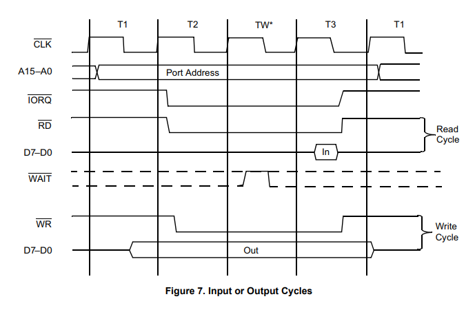
Note when the Z80 is writing, the Address and Data lines are stable for around a 1/2 clock period after the IORQ and WR signals have transitioned to their high inactive state.
This is important for any I/O device that latches data on the positive edge of the WR signal. Such devices may require the Address and Data signals to be ‘held stable’ for some period of time after the WR signal goes high. The 512K ROM/RAM module use the 74HCT670 IC to control memory banking, and this chip requires about 5ns of hold time when the WR signal transition to high. For a Z80 at a clock frequency of 20Mhz, half a clock will equate to about 25ns, so we are well within the specification of the chip.
Now, lets look at the timing diagram for the eZ80 running in Z80 Bus Mode.
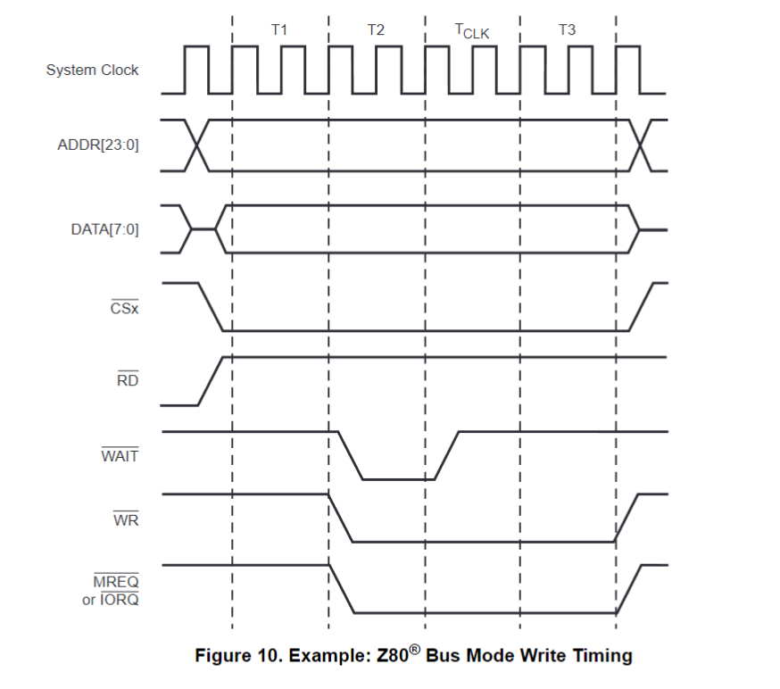
As the CPU is running in Z80 Bus Mode, multiple CPU clock signals will equate to one ‘T-STATE’ period. By choosing a ratio of 3 or 4 clocks per T-STATE, we ensure that the I/O read and write operation occurs over a duration that will tend to be within tolerances of any connected devices.
But have a look at when the Address and Data signals are released as the WR signal goes high. The Address and Data lines are released almost immediately after the WR signal goes high. No numbers are shown, but the diagram does seem to indicate a small delay is incurred between WR going high and the Address and Data lines being released. My experiments seem to indicate we are right on the 5ns boundary.
I was only able to make the RAM/ROM paging I/O operations work, when I used 74HCT245 buffer chips for my eZ80 Bus Interface module and 74HC670 in the 512K ROM/RAM module. If I swapped the type of logic chips used in these modules, that is, I used 74HC245 for the buffer chips and 74HCT670 in the ROM/RAM module - then it would fail to work reliably (intermittent failures would happen).
The 74HCTxxx chip are very similar to 74HCxxx chips - their main difference is in the input voltage thresholds for high/low signals. But they can also have very slight difference in propagation and other timing differences - perhaps just a tiny few nanoseconds.
So it seems there is just enough difference in timing, such that when I swap the type of logic chips around I was moving from having just enough ‘hold’ time for the Address and Data, to not quite enough ‘hold’ time.
The fact that I have buffered all of the eZ80 signals (address, data, control), means we will get a small but important delay. The buffer chips will effectively hold the data signals for a little bit longer than the eZ80 will. Hence why the type of buffer chips used seems to have an impact in timing and operation.
This all suggested to me, that eZ80 is not providing the 74HCT670 with sufficient hold time, after WR goes high.
So I needed to figure out a way to increase the ‘Hold Time’ of the Address and Data signals, when WR transition to its high level, to ensure a wider compatibility.
Only way I could think of doing this, was to design a logic circuit that would create a new signal, WR (bus-wr), that goes low when the eZ80’s WR goes low, but transition to high before the eZ80 transitions its WR to HIGH. Something like this:
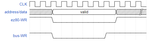
I would need the logic design to:
- Wait for eZ80-WR to go low.
- Make bus-WR go low.
- Start a logic counter from 0 (incrementing as the CPU clock ticks).
- When the counter reach the desired point, make bus-WR go high.
- when eZ80-WR goes high, restart and wait for the next low transition.
This requires a least a counter and a flip-flop. Given its getting a little crowded on the interface module PCB, I decided on using a single IC to achieve this function. I am using the Atmel ATF16V8C PLD (programmable logic device) to implement a counter and flip-flop to model the timing diagram above.
The new design has been assembled, PLD coded and programmed and the platform tested. And now finally, the 512K ROM/RAM Memory Module is working well within specification.
This enhancement should also help make other modules that might have similar timing issues work.
Another successful step in the goal of getting an eZ80 CPU to drive retro RC2014/RCBus modules!